Neurophos has raised $110 million to bring photonic computing to AI inference, betting that tiny metasurface modulators can deliver big gains in speed and energy efficiency. Spun out of Duke University and incubator Metacept, the Austin startup draws on metamaterials research that once enabled early “invisibility cloak” experiments and is now steering it toward the data center.
How Metamaterials Are Powering Next‑Gen AI Inference
The company’s core device is a metasurface modulator engineered to perform matrix–vector multiplications, the linear algebra at the heart of transformer inference. In essence, the modulator behaves like an optical tensor core: thousands of units are tiled onto a chip to process many operations in parallel using light rather than electrons.
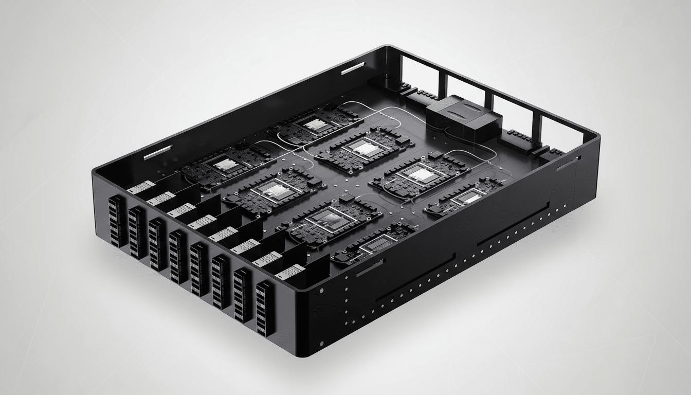
Neurophos argues that photons offer three advantages for AI workloads: minimal heat generation, high propagation speed, and resilience to electromagnetic noise. The challenge has always been density and manufacturability—optical components tend to be bulky, analog–digital conversions burn power, and yields can be unforgiving. The company claims its metasurface is roughly 10,000x smaller than traditional optical elements, enabling dense arrays that fit within standard chip footprints.
Performance Claims and the Power Math Behind Them
On paper, the performance targets are eye-catching. Neurophos says its optical processing unit runs at 56 GHz with a peak 235 peta-operations per second (POPS) while drawing 675 watts. By comparison, Nvidia’s B200 is cited at about 9 POPS at 1,000 watts. That implies a performance-per-watt uplift on the order of 39x (235/675 vs. 9/1000), assuming comparable operation definitions and low-precision arithmetic common in inference.
The company also projects roughly 50x gains in speed and energy efficiency over Blackwell-class silicon by its planned launch window, asserting an advantage that outpaces incremental node shrinks. It points to the historical cadence of leading-edge foundries—often mid-teens % efficiency improvements per node over multi-year intervals—as evidence that purely silicon-based progress is increasingly incremental.
Real-world throughput will hinge on more than raw POPS: memory bandwidth, nonlinear activation handling, model sparsity, and interconnect fabric all shape end-to-end latency. In most photonic accelerators, the optical array executes the linear layers while electronics handle activation functions and control. Neurophos says its approach is designed with this hybrid flow in mind.
Why This Matters for Data Centers and AI Scale-Out
Inference is becoming the dominant cost driver for AI services as deployed models serve billions of requests. The International Energy Agency has warned that data center electricity demand could roughly double over the next few years, with AI a material contributor. Any accelerator that delivers large efficiency gains without sacrificing accuracy stands to unlock capacity and cap operating costs for hyperscalers.
Neurophos contends its chips can be fabricated using standard silicon foundry materials, tools, and processes, a critical claim given the history of photonics startups constrained by bespoke manufacturing. If validated, that compatibility should simplify supply chain integration, packaging, and cost curves, especially as co-packaged optics and advanced substrates become mainstream in AI systems.
Backers and the Competitive Landscape in Photonics
The $110 million Series A is led by Gates Frontier with participation from Microsoft’s M12, Carbon Direct, Aramco Ventures, Bosch Ventures, Tectonic Ventures, Space Capital, and others. Microsoft technical leaders have publicly emphasized the need for step-change efficiency in core AI infrastructure, and the company is said to be evaluating the technology closely.
Neurophos enters a crowded arena anchored by Nvidia, whose GPUs power most of today’s training and inference. Several photonics players have shifted toward optical interconnects rather than full compute, including Lightmatter, while others such as Ayar Labs focus on optical I/O. Meanwhile, hyperscalers continue to push custom silicon for inference efficiency (e.g., TPU and Inferentia). To stand out, Neurophos must translate lab metrics into repeatable system-level gains on mainstream workloads.
Roadmap and What to Watch as Neurophos Scales Up
The fresh capital will fund an integrated photonic compute system spanning data center–ready OPU modules, a full software stack, and early-access developer hardware. The company is expanding in Austin and opening a San Francisco engineering site, signaling a push to recruit compiler, systems, and photonics talent.
Key milestones to monitor include developer toolchains that slot into existing workflows (think ONNX and PyTorch bridges), MLPerf Inference results, memory and I/O integration, and cost per deployed tera-op. Equally important will be evidence that the analog–digital boundaries do not erase the promised efficiency gains when scaled to model sizes used in production.
If Neurophos can deliver even a fraction of the projected performance and power advantages at volume, photonic compute could move from research curiosity to a practical accelerator tier. The metamaterials journey from cloaking experiments to AI chips underscores a broader trend in computing: the next leap may come not from a smaller transistor, but from rethinking the physics that do the math.