


In a high-volume SMT line producing dense IoT sensor boards, we once watched first-pass yield drop nearly eight points overnight. The culprit was not placement accuracy or paste volume—it was an outdated inspection program that generated so many false calls operators began overriding them. That experience is common across factories. Automated Optical Inspection only delivers value when the program itself is engineered with the same rigor applied to the board design. Effective AOI programming turns a camera system into a process control tool rather than a source of noise.
Why Programming Discipline Matters More Than Hardware Specs
Modern AOI platforms offer impressive resolution and 3D profiling. Yet the best hardware still fails when the inspection criteria do not match real process variation. Electrical engineers specify fine-pitch BGAs and 01005 passives; manufacturing engineers must translate those specifications into measurable optical thresholds. Without that translation, the system either misses critical bridges or floods the line with nuisance stops.
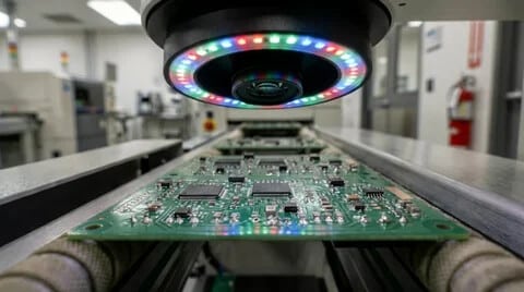
From the process-control perspective, three factors dominate long-term performance:
- Accurate geometric reference data imported from CAD and Gerber
- Lighting and focus settings that remain stable across board lots
- Tolerance windows that reflect actual process capability rather than theoretical maximums
When these elements are aligned, AOI becomes the earliest reliable feedback loop after reflow.
Core Elements of a Production-Ready Inspection Program
A robust program begins long before the first board enters the machine. Data preparation sets the foundation. Import complete Gerber, drill, and netlist files so the software can reconstruct the intended copper and component geometry. Verify that every custom footprint in the library matches the physical part—especially polarity marks and pin-1 indicators. Incomplete libraries remain one of the most frequent root causes of systematic false calls.
Fiducial teaching follows. Select at least two global fiducials and, on larger panels, local fiducials near critical areas. The software calculates board stretch and rotation; any residual error here propagates into every subsequent measurement. Board outline definition must exclude keep-out zones such as heat sinks or tall connectors that would otherwise trigger unnecessary inspections.
Component and solder-joint rules are then applied. Presence/absence checks use area or pattern matching. Placement offset and rotation tolerances are set according to IPC class requirements. For solder joints, 2D systems rely on fillet shape and color; 3D systems add height and volume data. The distinction is critical: a 2D-only program cannot reliably quantify insufficient solder on hidden joints, while a 3D program can.
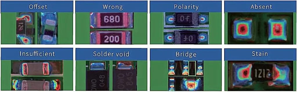
Practical Tolerance Comparison for Common Defect Types
The following table summarizes typical acceptance windows used on Class 2 and Class 3 products in high-mix factories. These values are starting points; final thresholds are always validated against actual process data.
| Defect Category | Class 2 Typical Limit | Class 3 Typical Limit | Factory Adjustment Guidance |
|---|---|---|---|
| Component X/Y offset | ±0.10 mm | ±0.05 mm | Expand slightly for flexible substrates |
| Component rotation | ±5° | ±2° | Tighten after fiducial variance is confirmed |
| Solder bridge height | < 0.05 mm | < 0.03 mm | Combine with color correlation on 3D systems |
| Fillet coverage | > 75 % pad area | > 90 % pad area | Cross-check with SPI paste volume trends |
| Missing component | Area match < 90 % | Area match < 95 % | Add polarity verification for polarized parts |
These numbers illustrate why a single generic program rarely works across product families. A Class 3 medical board demands tighter windows; applying the same windows to a cost-sensitive consumer product generates excessive false calls and slows the line.
Optimization Practices That Survive Real Production
Once the initial program is created, validation begins with known-good and known-bad boards. First-article inspection compares every AOI call against manual microscopic review. Discrepancies are logged and thresholds adjusted iteratively. False-call rate is tracked daily; most factories target less than 0.5 % of inspected boards requiring operator review.
Additional practices proven on the floor include:
- Storing separate programs for each panel size and board revision to avoid accidental reuse of obsolete data
- Integrating AOI results with the manufacturing execution system so defect trends can be correlated with stencil printer or placement machine offsets
- Using machine-learning modules available in newer software to propose threshold changes based on historical good and bad boards
- Applying 3D compensation algorithms when boards exhibit warpage greater than 0.5 % of diagonal length
For multi-layer rigid boards, surface AOI is often supplemented by bare-board optical inspection of inner layers. This dual approach catches copper defects that would otherwise escape until functional test. Early coordination with a PCB partner during data preparation further reduces the chance of mismatched Gerber or footprint libraries reaching the inspection stage.
Troubleshooting Recurring Program Issues
Reflections from shiny solder or conformal coating remain a frequent source of false positives. Increasing diffuse lighting or adding polarizing filters usually resolves the problem. Missed defects often point to insufficient resolution or outdated focus calibration. Component lot variation—especially color differences in molded packages—requires library updates rather than wider tolerances. Warped panels benefit from real-time 3D height mapping before inspection begins.
Root-cause discipline is essential. Every escape or false call should be traced to a specific programmable parameter. Over time this data reveals whether the issue belongs to design, process, or inspection programming itself.
Closing Perspective
AOI systems are only as capable as the programs that drive them. By treating program creation as an engineering activity—complete with data integrity checks, class-specific tolerances, and continuous validation—manufacturers convert optical inspection from a bottleneck into a reliable process-control asset. The result is fewer escapes, lower rework cost, and clearer feedback to design and process teams. Factories that invest in disciplined programming consistently achieve the yields their customers expect, even as component density and product mix continue to increase.