


Custom plastic parts form the backbone of modern electronics, from smartphone housings to industrial control enclosures. Every connector interface, every mounting point, and every shielding cavity depends on molded components that meet exacting dimensional standards. Yet scaling from prototype to high-volume production introduces manufacturing pitfalls that can silently compromise PCB performance and overall product reliability. Warped enclosures misalign critical connectors. Inconsistent material properties degrade signal integrity in high-speed circuits. Shrinkage variations disrupt carefully planned PCB layouts, turning a validated design into an assembly nightmare.
These failures rarely stem from a single cause. They emerge at the intersection of injection molding processes, PCB layout decisions, PCBA engineering constraints, and signal integrity requirements. Preventing them demands a coordinated approach that bridges the gap between mechanical and electrical disciplines from the earliest design stages through full-scale production. This article delivers practical solutions for electronics manufacturers seeking to eliminate these costly pitfalls, maintain manufacturing reliability at scale, and ensure that every molded part supports—rather than undermines—the electronics it protects.
- 1. The Fundamentals of High Volume Custom Plastic Injection Molding
- 2. Critical Pitfalls Linking Molding to PCB and PCBA Failures
- 3. Designing for Reliability: Integrating Molding with PCB Requirements
- 3.1. Optimizing PCB Layout for Molded Enclosures
- 3.2. PCBA Engineering Considerations for Molded Parts
- 4. Step-by-Step Solutions to Prevent Manufacturing Pitfalls
- 4.1. Phase 1: Pre-Production Planning and Design Review
- 4.2. Phase 2: Tooling and Process Optimization
- 4.3. Phase 3: Quality Assurance and Continuous Monitoring
- Achieving Scalable Precision Through Integrated Molding and Electronics Design
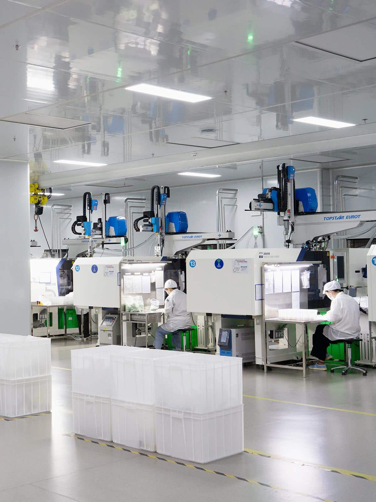
1. The Fundamentals of High Volume Custom Plastic Injection Molding
High-volume custom plastic injection molding refers to the production of thousands to millions of precisely engineered plastic components tailored to specific product requirements. In electronics manufacturing, these parts serve as enclosures, structural supports, connector housings, and EMI shielding cavities that directly interface with printed circuit boards. The process involves injecting molten thermoplastics—commonly ABS, polycarbonate, or glass-filled nylons—into precision-machined steel molds under controlled temperature and pressure conditions.
The transition from prototyping to mass production represents a critical inflection point. A design that performs flawlessly in small batches can develop subtle defects when cycle times accelerate and cavity counts multiply. Thermal dynamics shift in multi-cavity molds, gate locations influence fill patterns differently at production speeds, and material lot variations introduce property fluctuations that prototype runs never reveal. Each of these factors compounds when the molded part must maintain dimensional tolerances tight enough to support downstream PCB assembly. A mounting boss that shifts by 0.15mm may seem insignificant in isolation, but across an enclosure with twelve board-mounting points, that variation can induce mechanical stress on solder joints, misalign press-fit connectors, or compromise the sealing geometry around sensitive RF sections. Understanding these fundamentals establishes why precision in molding directly determines success in electronics integration.
2. Critical Pitfalls Linking Molding to PCB and PCBA Failures
High-volume injection molding introduces failure modes that ripple directly into electronics performance. Warping ranks among the most destructive—when enclosure walls bow even slightly due to uneven cooling or residual stress, PCB mounting surfaces lose planarity. Boards forced into warped housings experience flexural stress that fractures solder joints over time, particularly on BGA packages where crack propagation remains invisible until field failure. Shrinkage presents equally insidious challenges. Thermoplastics shrink between 0.4% and 2% depending on material and processing conditions, and this shrinkage rarely occurs uniformly. Differential shrinkage between thick and thin wall sections shifts boss positions, alters snap-fit geometries, and changes the internal cavity dimensions that define clearances around populated circuit boards.

Material inconsistencies across production lots compound these geometric problems. Variations in filler content, moisture absorption characteristics, or crystallinity levels alter both mechanical and electrical properties of the molded part. Tooling design pitfalls further erode reliability—poorly positioned gates create weld lines in structurally critical areas, inadequate venting causes burn marks near EMI shielding surfaces, and insufficient draft angles make ejection forces deform precision features. Each defect category connects directly to downstream electronics failures, making early identification essential for maintaining production quality across extended runs.
2.1. Impact on PCB Layout and Assembly
When molded dimensions drift outside specification, the carefully planned spatial relationships between PCB components and enclosure features break down. Mounting holes that shift relative to each other force boards into stressed positions, altering component-to-wall clearances that thermal engineers calculated for adequate heat dissipation. Connector cutout misalignment creates insertion force problems during PCBA assembly, potentially damaging both the connector and its solder connections. Thermal management suffers when gap pad interfaces lose their designed compression because enclosure surfaces no longer sit at predicted distances from heat-generating components.
2.2. Risks to Signal Integrity and Performance
Molded enclosure materials directly influence high-frequency signal behavior through their dielectric properties. When material lot variations shift the dielectric constant, antenna chambers tuned for specific frequencies detune, and near-field coupling between traces and enclosure walls changes unpredictably. Physical defects like internal voids or density variations near shielding cavities create inconsistent electromagnetic environments, introducing impedance discontinuities in transmission lines routed close to enclosure surfaces. Weld lines in RF compartment walls act as slots that leak electromagnetic energy, compromising isolation between circuit sections designed to operate independently.
3. Designing for Reliability: Integrating Molding with PCB Requirements
Preventing molding-related electronics failures requires deliberate integration between mechanical and electrical design teams from project inception. The most effective approach establishes shared design constraints before either discipline finalizes its geometry. Molding engineers need visibility into critical PCB mounting locations, connector positions, and RF-sensitive zones, while PCB layout designers need accurate shrinkage predictions, achievable tolerance bands, and material property data for the specific resin grade selected for production. This collaborative framework eliminates the costly iteration cycles that occur when teams work in isolation and discover incompatibilities during first-article inspection.
Material selection represents a pivotal decision point where electrical and mechanical requirements must be balanced simultaneously. For enclosures housing high-speed digital circuits or RF subsystems, the resin's dielectric constant, loss tangent, and their stability across temperature and humidity ranges matter as much as mechanical strength or flame rating. Glass-filled materials offer dimensional stability but introduce anisotropic shrinkage that complicates tolerance prediction. Unfilled resins shrink more uniformly but may lack the stiffness needed to maintain flatness across large mounting surfaces. Resolving these tradeoffs early—through simulation-guided material screening and targeted prototype validation—prevents discoveries during production ramp that force expensive tooling modifications or PCB redesigns.
3.1. Optimizing PCB Layout for Molded Enclosures
PCB layout should incorporate molding tolerance bands as explicit design constraints rather than afterthoughts. Place critical components with clearance margins that account for worst-case enclosure dimension shifts—typically adding 0.2–0.3mm beyond nominal clearances for features dependent on molded references. Route high-speed differential pairs away from enclosure walls where dielectric variations could affect impedance, and position mounting holes to allow slight board float rather than over-constraining the assembly. Keep thermally sensitive components away from areas where enclosure thickness transitions create localized hot spots during operation.
3.2. PCBA Engineering Considerations for Molded Parts
PCBA assembly sequences must account for the mechanical reality of molded parts under production variation. Design snap-fit and screw-boss interfaces to provide compliance rather than rigid constraint, distributing assembly forces across multiple attachment points so that no single solder joint bears mechanical load. Specify assembly torque limits calibrated to the creep characteristics of the chosen resin, and incorporate thermal relief features where heat-generating components contact molded surfaces. These measures ensure that normal molding variation does not translate into cumulative mechanical stress that degrades solder joint reliability over product lifetime.
4. Step-by-Step Solutions to Prevent Manufacturing Pitfalls
Eliminating manufacturing pitfalls in high-volume custom molding requires a structured, phased approach that treats mechanical and electrical integration as inseparable throughout the product lifecycle. Rather than addressing molding quality and electronics performance as separate concerns, effective prevention embeds signal integrity verification, dimensional validation, and assembly compatibility into every stage from initial design through sustained production. Experienced molding manufacturers like WEILAN MFG emphasize this integrated methodology, recognizing that process control must be driven by end-use electronics requirements rather than mechanical tolerances alone. The following framework provides electronics manufacturers with concrete actions organized into three phases—each building upon the previous to create a robust defense against the defects that compromise PCB performance at scale.
4.1. Phase 1: Pre-Production Planning and Design Review
Begin with a joint DFM analysis that evaluates both moldability and electronics integration simultaneously. Map every PCB-to-enclosure interface—mounting bosses, connector apertures, shielding walls, thermal contact zones—and assign tolerance budgets based on achievable molding capability rather than ideal geometry. Conduct a cross-functional design review where molding engineers, PCB layout designers, and PCBA process engineers collectively identify risk areas. Flag features where shrinkage-induced dimensional shift could affect signal integrity, such as antenna cavity walls or impedance-controlled trace routing zones near enclosure surfaces. Document material dielectric requirements alongside mechanical specifications so that resin selection satisfies both disciplines before tooling commitment.
4.2. Phase 2: Tooling and Process Optimization
Invest in mold flow simulation before cutting steel, optimizing gate locations to eliminate weld lines in EMI-critical zones and ensuring balanced fill across all cavities. Design cooling circuits to minimize differential shrinkage at mounting boss clusters and connector openings. Establish process windows with scientific molding principles—characterize viscosity curves, determine optimal pack-and-hold profiles, and validate dimensional stability across the full operating range of barrel temperatures and cycle times. Tie critical-to-quality dimensions directly to PCBA assembly requirements, ensuring that process control limits reflect what electronics integration actually demands rather than arbitrary mechanical tolerances.
4.3. Phase 3: Quality Assurance and Continuous Monitoring
Implement in-process measurement systems that track critical dimensions in real time, using cavity pressure sensors and automated vision inspection to detect drift before it produces nonconforming parts. Conduct periodic signal integrity validation on assembled units, measuring antenna performance, shielding effectiveness, and impedance consistency to confirm that molding variation remains within electrically acceptable bounds. Establish statistical process control charts linked to electronics-relevant quality metrics, and define corrective action triggers that initiate investigation before dimensional trends reach limits that would affect PCB assembly yield or field reliability.
Achieving Scalable Precision Through Integrated Molding and Electronics Design
High-volume custom plastic injection molding for electronics demands more than mechanical precision—it requires a holistic integration of molding processes with PCB layout, PCBA engineering, and signal integrity disciplines. The pitfalls that compromise product reliability at scale—warping, shrinkage variation, material inconsistencies, and tooling defects—never exist in isolation. They propagate through the entire electronics assembly, manifesting as misaligned connectors, stressed solder joints, degraded RF performance, and premature field failures that erode customer confidence and inflate warranty costs.
Manufacturers who adopt the proactive, phased approach outlined here—embedding cross-functional collaboration into pre-production planning, optimizing tooling with electronics requirements as primary constraints, and maintaining continuous quality monitoring tied to electrical performance metrics—position themselves to scale production without sacrificing the precision that electronics demand. The upfront investment in simulation, scientific molding characterization, and integrated design reviews pays dividends through higher first-pass assembly yields, fewer field returns, and faster time to volume production. By treating every molded enclosure as an active participant in electronics performance rather than a passive container, manufacturers build products that deliver consistent reliability across millions of units while reducing the total cost of quality over the product lifecycle.