PowerLattice — a newish semiconductor startup specializing in power delivery — has attracted investment from former Intel CEO Pat Gelsinger, who is currently a general partner at Playground Global. The company came out of stealth mode with a $25 million Series A led by Playground Global and Celesta Capital, for a total of $31 million in funding, and a power-saving chiplet that it said can reduce system power requirements by more than 50%.
The pitch is easy to articulate and devilishly challenging: get power regulation a lot closer to the compute die, greatly reducing conversion and distribution losses that sap energy from today’s AI hardware and data centers. The support of a leader who was running the world’s largest chip maker, at that time, is also an indication that the idea might be ready for prime time.
Why Power Delivery Is The Limiting Factor
Now that the current rush of AI accelerators are knocking on 500–700 W per device and racks are in the range of 30–100 kW, delivery mechanisms to supply stable and efficient power to the silicon have become as important as adding more FLOPs. Average data center PUE (Power Usage Effectiveness) has remained mired in the mid‑1.5 range or above, according to Uptime Institute. IEA also warned that global data center electricity use could nearly double by 2026, with AI a big culprit. Real cuts in conversion and distribution losses trickle down to total energy bills, cooling load, and infrastructure size.
With board‑level VRMs, traditional power delivery passes a high current load through crowded and long interconnects to the CPU, leading to electrical (IR) losses that manifest in wasted energy and higher temperatures that scorch CPUs under heavy workloads such as AI applications.
PowerLattice’s chiplet is trying to do high‑efficiency conversion on‑package or at least near‑die, and shave all these resistive paths and render the transient response better, which can also allow you to avoid using massive decoupling capacitors. It’s an elaboration on the integrated voltage regulation ideas seen in previous CPUs, reimagined for the multi‑chip module age we live in today.
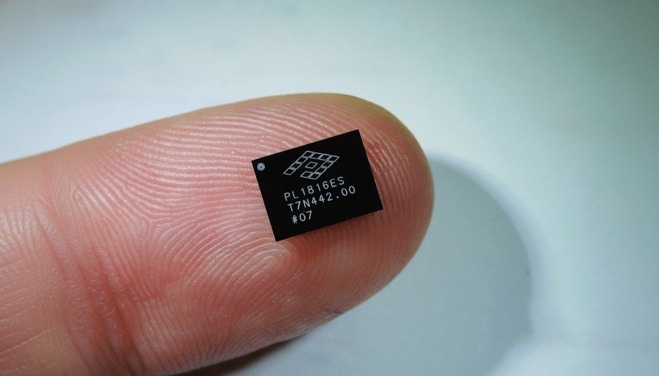
Funding And Early Manufacturing Plans At TSMC
PowerLattice, created in 2023 by veterans from Qualcomm, NUVIA and Intel, says its first chiplets are already being fabbed at TSMC. Early silicon is being verified by an undisclosed manufacturer, and broader customer evaluations are expected in 1H26, the company added. That time frame coincides with hyperscalers’ investments in next‑gen AI systems that depend more and more on advanced packaging, including 2.5D interposers and high‑density chiplet integration.
Gelsinger’s participation is through Playground Global, which co‑led the round with Celesta Capital. The imprimatur is significant: investors and chip designers alike tend to view power delivery as a high‑stakes, failure‑intolerant domain. A credible route from prototype to volume production — particularly on a TSMC node in limited supply — can be the difference between an exciting lab demo and a design‑win in a flagship accelerator board.

Who Might Buy This Chiplet, And Why It Matters
PowerLattice’s potential customers read like an industry who’s who of AI silicon: established players such as Nvidia, AMD, and Broadcom, along with a handful of specialized startup names you’ve probably never heard of — Cerberus, Groq, d‑Matrix and NextSilicon. Even if the biggest vendors keep in‑house power teams, a packaged, proven chiplet that saves board area, simplifies VRM design, and boosts performance per watt can be convincing — particularly as it is power limits — not raw compute — which are increasingly setting capacity constraints for systems.
The economics are straightforward: losses translate into larger cooling plants, more copper, and less rack density. Stanching those losses at the chip level by a purported 50% can add up to big changes in total cost of ownership for AI clusters, where power and cooling are often the dominant operating expense. And for cloud operators moving to 48 V distribution and Open Compute–style designs, on‑package conversion lines up with the direction of a higher‑voltage, efficient power path.
Competitive Landscape And Key Risks For Adoption
PowerLattice is not alone. One such example is Empower Semiconductor, which has raised a substantial war chest and aims at point‑of‑load power with high‑density, fast regulators. The rest of the ecosystem, from Karim’s company Vicor to board‑level VRM suppliers, is also bidding for affection with efficiency‑first solutions. It’s going to be how cleanly your chiplet integrates into existing multi‑die packages without cratering thermal budgets, bump maps, or yields.
Then there is the issue of measurement. A 50% improvement might mean many different things at different points in the chain: converter efficiency, end‑to‑end delivery losses, or system‑level power draw under workload. Smart buyers will insist on apples‑to‑apples data spanning real AI inference and training profiles, including transient behavior and hot‑spot thermals. If the figures stick, the payoff could be big.
What Comes Next For PowerLattice’s Chiplet Ambitions
If early TSMC runs indeed prove the claims, funds to finance production and customer support could very quickly jump in size. Advanced packaging capacity is constrained, so winning line time and reliable assembly flows will be as crucial as the chiplet’s electrical performance. Design‑wins in a high‑volume accelerator can help establish a beachhead and create a positive cycle of board simplification and system‑level energy savings.
For now, the headline is all but written: PowerLattice has the money and a manufacturing partner — not to mention the ear of one of industry’s most influential figures. At a time when power, not transistors, is the ultimate limiter of progress, a smart power‑delivery chiplet could prove to be the well‑concealed keystone of the next wave in AI hardware.