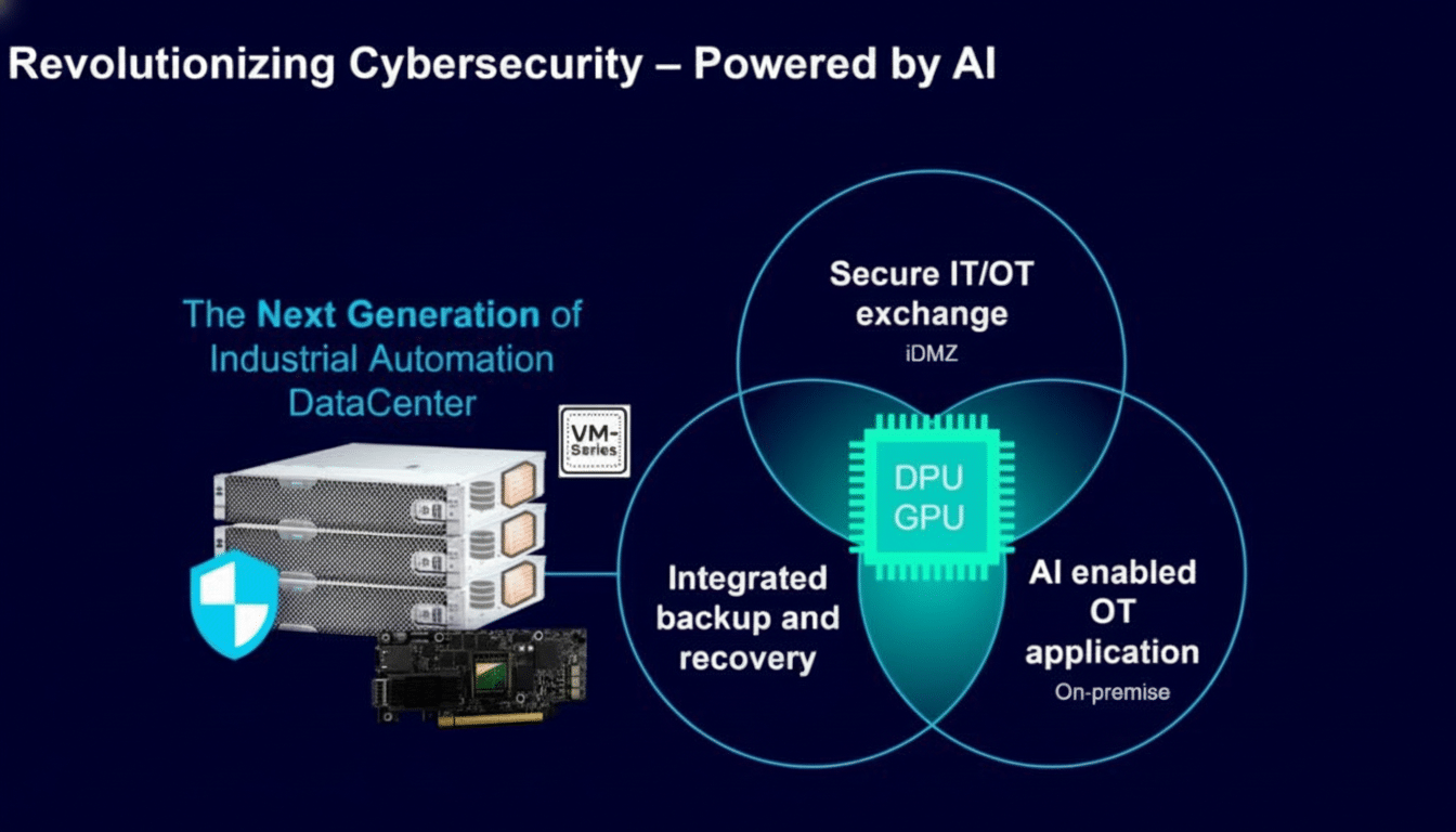
Nvidia is partnering with Siemens to use the German company’s electronic design automation tools on Nvidia GPUs — a potential way to reduce simulation times, lower energy consumption, and speed signoff for advanced semiconductors. The collaboration, announced at CES, addresses the most compute‑intensive stages of chip design and includes both digital simulations and fast‑running digital twins that model systems — from a single die up to system levels such as an entire data center rack.
Why GPU acceleration is important for modern EDA
Modern systems-on-chip now exceed 100 billion transistors, and that complexity strains verification, parasitic extraction, and electromagnetic analysis to the limits of CPU clusters. The ESD Alliance, a SEMI technology community, said quarterly electronic system design sales have surpassed $4 billion in 2024 — evidence that demand for compute‑intensive design software is driving growth with each new process node.

GPUs are an ideal candidate for the numerical kernels at the core of signoff workloads: sparse matrix factorizations in SPICE, 3D field solvers for power and signal integrity, and massive Monte Carlo sweeps across corners. As industry peers have already shown the way, vendors report “up to 10x speedups on GPU‑accelerated circuit simulation and extraction,” so getting Siemens EDA onto Nvidia’s CUDA ecosystem could directly yield such gains (while reducing queue times on their shared farms).
Which Siemens EDA tools are likely to benefit most
Siemens’ portfolio includes front‑end and signoff Calibre for DRC/LVS, advanced RET, mPower for EM/IR analysis, Aprisa for digital implementation and Questa verification as well as Xpedition PCB. There are clear heavy hitters when it comes to GPU offload. Calibre’s polygon operations, pattern matching, and lithography-aware checks are all well suited to parallel processing; mPower’s vector‑based dynamic IR and EM uses large linear algebra kernels but can be mapped naturally into the GPU memory hierarchies; mixed‑signal simulation in Symphony can employ GPU‑accelerated SPICE engines for analog blocks surrounded by digital functions.
Not every algorithm benefits equally. HDL simulation is branchy and latency‑sensitive in the event‑driven context, making blanket GPU acceleration more tricky. However, formal verification subproblems, coverage analysis, and waveform post‑processing can be executed as GPU‑accelerated data‑parallel pipelines. Trickle from the largest, longest‑running kernels and major features down, and iterate sideways into adjacent stages once determinism and signoff equivalence are locked.
Digital twins spanning chips, packages, boards, and racks
In addition to accelerating design closure, the companies aim to create digital twins across chips, packages, boards, and fully populated racks. Siemens’ Xcelerator and Simcenter suites combined with Nvidia’s Omniverse can connect EDA signoff results to multiphysics models for thermals, airflow, vibration, and power delivery. That allows real‑world constraints, like liquid cooling and 48V delivery, to be “shift‑left” validated well before there is any hardware to test on.
That matters for hyperscalers putting 100 kW+ in a rack. Hot spots, server‑level fan curves, and facility‑level cooling are influenced by a chip’s floorplan and placement of vias to the package. A linked twin allows teams to virtually validate firmware throttling strategies, PDN margin, and serviceability trade‑offs, allowing bring‑up cycles to be compressed and costly surprises on the lab bench to be avoided.

Industry background and competitive landscape
Nvidia’s entry comes into a market already exploring heterogeneous compute for EDA. Rival toolmakers have demoed GPU‑accelerated SPICE, extraction, and 3D EM solvers along the way, claiming order‑of‑magnitude run‑time reductions and lower energy per job. Foundries such as TSMC and Samsung have stepped up to support these efforts by certifying GPU‑enabled signoff flows at advanced nodes, where RET complexity and rule decks have grown substantially.
The bottleneck is no longer just raw FLOPS. Memory size and bandwidth, interconnect latency, and determinism all dictate whether signoff is possible or not. In this case, with GPUs and fast interconnects like NVLink, high‑performance memory can make large matrices and field meshes resident between steps, assuaging I/O churn. The result is a much better match for capacity‑limited problems — like full‑chip extraction, or voltage drop over massive power grids.
What this collaboration means for chipmakers and teams
Time‑to‑market is the headline benefit. If GPU‑enabled Calibre or mPower reduces a days‑long job to mere hours, design teams can iterate on timing, area, and power more aggressively. That multiplies across corners and ECO loops. And there’s a cost angle, too: shaving off runtimes reduces peak CPU core counts, releases expensive licenses sooner, and can decrease the energy per signoff step — vital as engineering teams chase sustainability initiatives.
Adoption won’t be push‑button. Teams will demand foundry‑quality correlation, hardware repeatability, and clear direction on job partitioning between CPU and GPU. But the payoff is where the effort goes: according to Wilson Research Group’s surveys, verification consumes 60–70% of project manpower. And compressing that tail — even a little bit of it — can free up schedules and budgets.
In brief, Nvidia’s collaboration with Siemens places GPU acceleration at signoff and system modeling. If the companies achieve predictable speedups on real production decks and path all the chip models into plausible rack‑scale twins, the impact will reach beyond banner runtimes to how we co‑design silicon, packages, and systems.

