The semiconductor industry continues to accelerate at a remarkable pace, driven by shrinking device geometries, greater performance expectations, and increasingly stringent purity requirements. As fabrication processes evolve, the need for ultra-clean materials and precise contamination control has never been more critical.
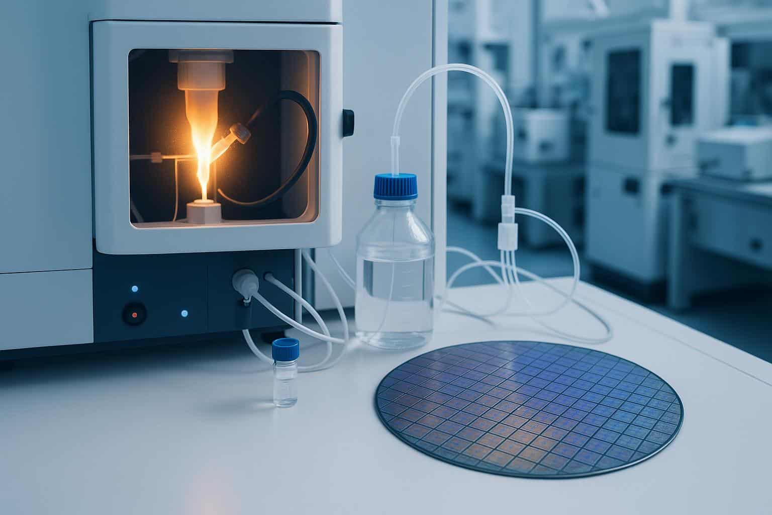
Among the advanced analytical techniques supporting this progress, Inductively Coupled Plasma Mass Spectrometry (ICP-MS) stands out. Through ICP-MS Analysis for Semiconductor Cleaning & Surface Preparation, manufacturers can detect and quantify trace metallic impurities at extremely low levels, ensuring that surfaces, chemicals, and process tools meet exacting purity specifications. This level of insight enables fabs to identify contamination sources early, improve yield, and support the production of next-generation semiconductor devices.
Why trace metal control matters
In semiconductor fabrication, the presence of metallic contamination, even at extremely low levels, can lead to reduced yields, device defects, and reliability issues. Contamination is estimated to account for more than half of yield losses in integrated circuit device manufacturing.
These contaminants can arise from multiple sources: wafer substrates, process chemicals such as etchants and solvents, ultrapure water, the ambient equipment environment, and deposition or lithography steps. As device feature sizes shrink to the single-digit nanometre scale, the tolerance for impurities becomes increasingly tight. Even parts per trillion (ppt) levels of a given metal can influence dielectric breakdown, leakage currents, or film adhesion.
What ICP-MS brings to the table
ICP-MS offers a suite of advantages that align with the rigorous demands of semiconductor process control:
- Ultra-low detection limits: Modern ICP-MS systems can detect trace metals at ppt or even sub-ppt levels in properly prepared samples. Some studies have shown detection limits as low as 0.03 µg/g for certain elements.
- Multi-element capability: Because multiple metallic contaminants must be screened simultaneously (such as Na, K, Ca, Fe, Cu, Ni), ICP-MS’s ability to analyse many elements in a single run is highly advantageous.
- Rapid, high-throughput analysis: Wafer surface methods using surface metal extraction (SME) combined with ICP-MS can enable sample preparation and analysis in under 20 minutes, providing near-real-time monitoring of manufacturing steps.
- Flexible sample types: ICP-MS can handle a wide range of sample matrices, from dissolved wafers and liquids such as ultrapure water, acids, and solvents, to surface extraction techniques like vapour-phase decomposition or droplet analysis.
Specific applications in semiconductor manufacturing
- Wafer substrate contamination assessment: The silicon wafer and its surface layers — including oxides and films — must be virtually free of metallic impurities. ICP-MS enables detection of trace metals introduced during wafer slicing, polishing, or oxidation. Techniques like vapour-phase decomposition allow surface metals to be extracted and analysed accurately.
- Process chemicals and reagent monitoring: Every process chemical, from strong acids to organic solvents and ultrapure water, must meet stringent impurity specifications (often less than 100 ppt or even 10 ppt for each trace metal). ICP-MS ensures these chemicals comply with industry purity standards and that contamination risks are controlled.
- Ultrapure water (UPW) and rinse waters: The water systems used for rinsing wafers must also be monitored. ICP-MS provides an ideal solution for detecting trace metals in UPW systems, enabling early intervention before contamination affects production yields.
- Specialty gases and volatile liquids: In advanced manufacturing steps, high-purity gases and volatile liquids are used. When coupled with gas chromatography, ICP-MS can measure ultra-trace elemental impurities in these compounds, ensuring process integrity.
Benefits to semiconductor manufacturers in Australia and globally
For Australian semiconductor and micro-electronics manufacturers — as well as suppliers to global fabrication facilities — leveraging ICP-MS for trace metal control provides clear benefits:
- Improved yield and reduced cost – Detecting contamination early prevents costly yield losses, rework, and material waste.
- Competitive edge in purity – Meeting ultra-tight impurity specifications differentiates manufacturers in high-reliability sectors like automotive, defence, and medical electronics.
- Regulatory and quality assurance compliance – Robust trace metal control supports certification, compliance, and customer confidence.
- Adaptability to new materials and technologies – ICP-MS is well suited to emerging materials such as silicon carbide (SiC) and gallium nitride (GaN), providing a versatile analytical foundation for future processes.
Challenges and considerations
While ICP-MS is a powerful tool, manufacturers must consider several factors to achieve reliable results:
- Sample preparation and contamination control – Achieving the lowest detection limits requires cleanroom conditions, ultra-pure reagents, and precise handling techniques.
- Matrix effects and interferences – Complex matrices like acids and organic solvents can introduce polyatomic interferences. Advanced systems such as triple-quadrupole ICP-MS help overcome these challenges.
- Cost and skill requirements – ICP-MS instruments and clean-lab facilities represent significant investments, requiring skilled analysts and ongoing quality control.
- Alignment with industry standards – Methods must align with SEMI and international standards to meet customer and regulatory expectations.
Conclusion
ICP-MS is a cornerstone of modern semiconductor trace metal analysis. Its unparalleled sensitivity, speed, and flexibility make it essential for maintaining purity and yield in advanced fabrication environments. For manufacturers focused on quality, reliability, and cost efficiency, ICP-MS-based trace metal control is not just an analytical tool — it’s a strategic investment in long-term success.