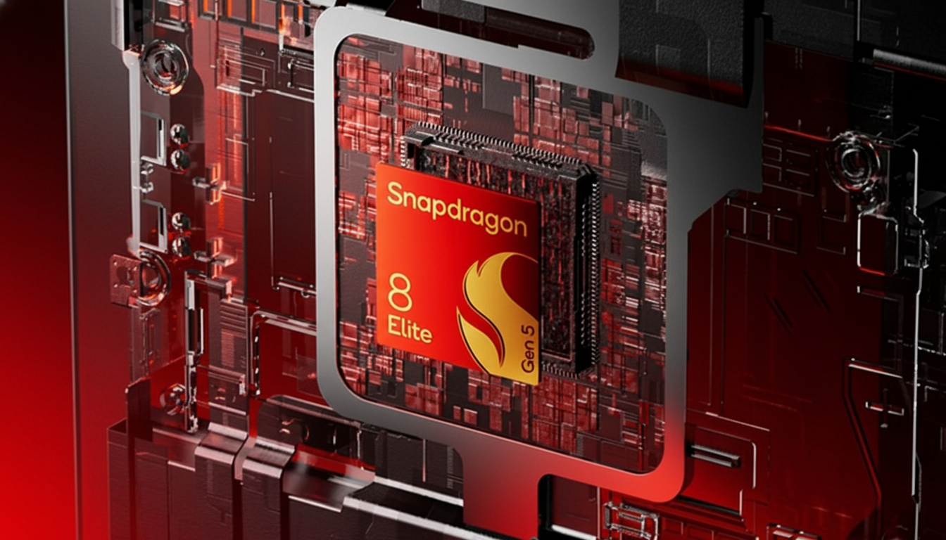
A new leak suggests that the next (likely named) Qualcomm smartphone flagship processor – the Snapdragon 8 Elite Gen 6 – is moving on to TSMC’s N2P process with some fancy memory and storage in tow. If true, the change could bring a massive surge in performance per watt to new phones and raise flagship phone prices even higher. In short, it appears to be a step in the right direction with some strings attached.
What the leak shows us about Snapdragon 8 Elite Gen 6
According to reliable tipster Digital Chat Station, the Snapdragon 8 Elite Gen 6 is aiming for TSMC’s N2P node, supporting LPDDR6 RAM and UFS 5.0 storage.
- What the leak shows us about Snapdragon 8 Elite Gen 6
- Why an N2P shift matters for Qualcomm’s next flagship
- LPDDR6 and UFS 5.0: Raising the performance ceiling
- The price and the reality for next-gen Android flagships
- Real-world impact for the next Android flagships
- Important caveats and limits of this early leak

The chip is rumored to be model number SM8975, which would make it a successor to the 8 Elite Gen 5’s SM8850.
Context matters. (Want the full specs on board?) The 8 Elite Gen 5 is built using TSMC’s N3P 3nm-class process and maxes out at LPDDR5X RAM and UFS 4.1 storage. Leaping to N2P and to more advanced memory tiers and flash would uplift bandwidth/efficiency across CPU, GPU, and AI workloads.
Why an N2P shift matters for Qualcomm’s next flagship
TSMC has already said that N2 (its inaugural nanosheet GAAFET node) “provides about 10 to 15 percent higher speed, or about 25 to 30 percent power reduction, versus N3E.” N2P is portrayed as a more capable variant, which ideally will be able to scrounge up some efficiency gains and frequency margin. Final numbers will depend on how Qualcomm puts the design of its own SoCs together, but that kind of leap can result in cooler sustained performance and longer battery life from high-demand apps.
Going to gate-all-around transistors also opens the door to new design trade-offs. Early yields on new nodes can be more challenging and thermal density can go up as average power comes back down. OEMs (or the silicon manufacturers themselves) will no doubt rely on larger vapor chambers and smarter scheduling to hold those peak clocks. The upside is evident for on-device AI: a more efficient node, and memory that is faster and that you can shove into the chip, should raise token throughput and lower latency for large-model inference without torpedoing battery life.
LPDDR6 and UFS 5.0: Raising the performance ceiling
Low-power double data rate (LPDDR6) has long been on the horizon and is poised to launch mobile memory speeds well beyond the 8,533–9,600 MT/s possible with LPDDR5X. That means more bandwidth for everything from high-FPS gaming to multi-frame HDR processing and generative AI pipelines that are increasingly limited by memory. It also typically enhances energy per bit, which translates to more work per joule when accompanied by an efficient SoC.
From what we’ve heard, UFS 5.0 is the natural successor to today’s UFS 4.x, aimed at better sequential and random throughput, lower latency, and more advanced power states. That can translate to faster app resumes, less time to install applications, and quicker burst capture. Components, though, are going in the opposite direction: TrendForce has revealed double-digit percentage rises for DRAM and NAND contract prices over a number of quarters now, and next-gen components rarely come cheaply.

The price and the reality for next-gen Android flagships
Advanced nodes are expensive. Wafers in the 3nm class sell for substantially more than legacy nodes and runs are expected to price out similarly at 2nm. Early yields are a pressure to push up effective cost per good die. Paired with more expensive LPDDR6 and faster UFS, that true “no‑compromise” flagship could push up a device’s bill of materials by tens or potentially even hundreds of dollars.
That pressure is met by a market that’s already drifting upscale. The share of the premium segment and average selling prices are growing as per Counterpoint Research. If the cost base of Qualcomm’s flagship SoC goes up again, you can expect that to be passed on at least in part by OEMs — or for top SKUs to just become ultra-premium tiers while lower trims sit on older silicon.
Real-world impact for the next Android flagships
For users, the reasons to celebrate are already material. A switch to N2P plus faster memory and storage, meanwhile, should result in smoother sustained gaming, speedier camera pipelines, and faster on-device AI-focused tasks such as real-time transcription, image generation, or complex photo edits. It’s likely that thermal envelopes will be more manageable under these normal loads even if the peaks of stress tests still hit throttling walls.
For OEMs, the calls only get harder. Do they eat the higher silicon and memory costs, or worse, trim features? Do they pursue thin-and-light designs or invite increased cooling to unleash sustained performance? Look for different answers from brands such as Samsung, Xiaomi, and OnePlus, as they tune according to regional pricing and user priorities.
Important caveats and limits of this early leak
This is still a leak, not a spec sheet. Digital Chat Station is a reliable leaker, although plans can change between engineering samples and commercial silicon. Qualcomm’s ultimate CPU topology, GPU architecture, NPU throughput, and modem features — as well as how aggressively partners clock the chip — will determine real-world outcomes.
If the rumors are true, then Snapdragon 8 Elite Gen 6 seems set to be a significant jump forward, especially in the areas of efficiency and memory bandwidth. Just be ready for the possibility that the best Android phones with it will also push new price ceilings.

